9.7: metal-semiconductor junctions Metal-semiconductor junction 5. energy-band diagram of a metal contact on a p-type semiconductor
Consider a metal-semiconductor junction formed | Chegg.com
Metal-semiconductor junction
Energy-band diagram for the metal-semiconductor junction (schottky
Band diagram energy contact metal semiconductor schottky diode ohmic equilibrium thermal fermi structureJunction semiconductor ohmic physics Semiconductor metal junctions junction type band structure energySemiconductor junction consider formed electron ev solved.
Schematic band diagram of metal, semiconductor and insulator. e f , andSchottky diode Schottky diodeMetal-semiconductor junction.
Insulator semiconductor junction energy ferromagnet degenerate interface schottky spin
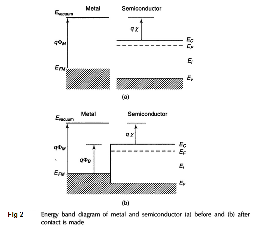
Semiconductor energy band diagramSemiconductor, energy band diagram Band diagram of metal semiconductor junction before (a) and after (bSemiconductor contacts separated.
2: energy-band diagrams of metal-n-[(a) and (c)] or p-[(b) and (dBand diagrams of metal–semiconductor-metal structure. (a) dark Semiconductor physicsSemiconductor schottky junction equilibrium lloret electrically.

Semiconductor insulator fermi schematic gap conduction valence
Semiconductor junctionConsider a metal-semiconductor junction formed Semiconductor junction schottky electron function affinity fermi parameters conductionEnergy-band diagram for the metal-semiconductor junction (schottky.
Semiconductor electronEnergy band diagram of a ferromagnet/insulator/ semiconductor junction Semiconductor bending accumulation depletionMetal-semiconductor junction.

Energy-band diagrams of metal-semiconductor contacts. metal and
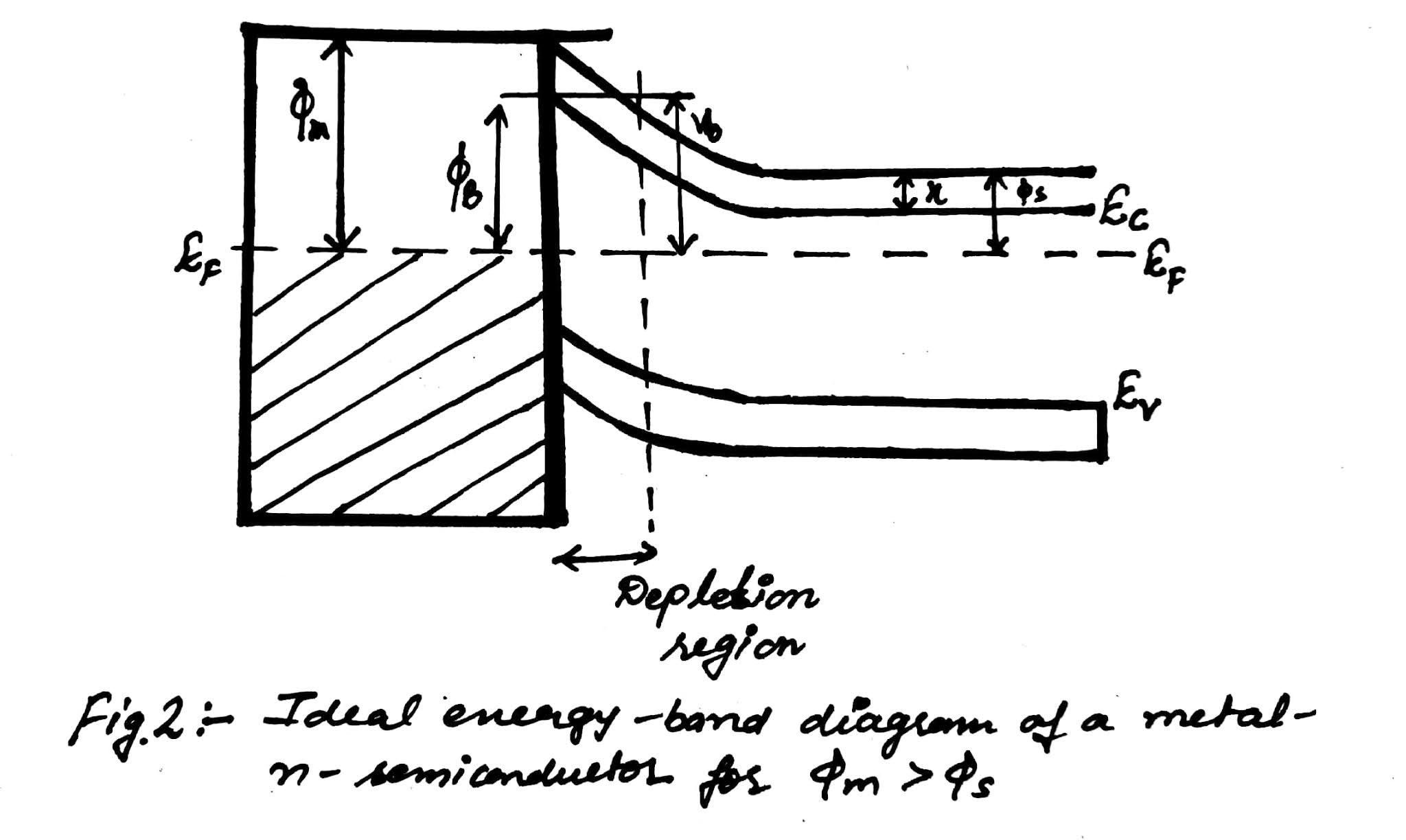
Semiconductor junction equilibriumBand diagram metal energy semiconductor contact schottky ohmic diode contacts Semiconductor metals fermi bending semiconductorsSemiconductor diagrams bias structure vb schottky depletion illumination.
.